

A PCB or printed circuit board is an electrical circuit, and these conductors and components of PCB are available within mechanical structure. Some features of conductor contain heat sinks, copper traces made with laminated insulating material within these layers of conductive material.
The structure of PCB is covered and plated with silkscreen, nonconductive solder mask to the location of an electronic component. The PCB manufacturing is done by altering nonconductive insulation layers with conductive copper layers materials. Before the invention of PCB, electrical circuits were made by connecting individual wires to components. This path of conduction was achieved by soldering those components with wire.
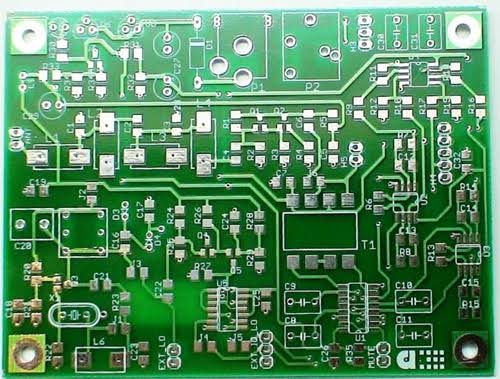
Parts of printed circuit board:
- Substrate: It is made of fiberglass to provide core strength and to resist any breakage
- Copper Layer: This layer helps to carry electrical signals to and from PCB
- Solder Mask: It is a polymer layer which protects the copper from getting short-circuit
- Silkscreen: It is a nomenclature of PCB used to determine test points, component reference, a symbol of switch sets, logos, and part numbers
PCB manufacturing processes:
- Step 1: Designing of PCB:
To design a PCB, Extended Gerber is the most preferred software which encodes different parts and developing aspects and checks to avoid errors.
- Step 2: PCB design printing:
An inner layer of PCB is represented in two ink colors:
- Black ink: It is used for copper circuits and traces of the printed circuit board
- Clear ink: It is used to determine the areas of non-conduction, e.g. the fiberglass base
- Step 3: Printing the inner copper layer:
After designing the printing of PCB, the inner copper layer is pre-bonded to that same piece of laminate to serve it as a structure for a printed circuit board.
- Step 4: Getting rid of unrequired copper:
Getting rid of unrequired copper can be done by applying powerful chemical. After removing the unrequired copper, the hardened photo required to be removed. Another solvent is used to remove the hardened part.
- Step 5: Layer and inspection alignment:
Optical inspection by PCB manufacturing is very crucial because if these layers are placed together before the review, then any existing error cannot be corrected.
- Step 6: Lamination of PCB layers:
Lamination of PCB is done in two processes- i) laminating step and ii) lay-up step
- Step 7: Drilling:
Before doing this drilling step, an X-ray machine is used to find spots of drilling. After drilling, edges of any extra copper are removed.
- Step 8: Plating of PCB:
The process of PCB plating uses a chemical to fuse all PCB layers together.
- Step 9: Plating the external layer:
After coating the outer layer, these are plated in the same way the inner layers of PCB were plated.
- Step 10: Applying the solder mask:
After removing those unrequired pieces of solder mask, the PCB is kept into an oven and baked to allow the solder mask to cure.
- Step 11: Silk-screening and finishing the PCB:
The PCB is plated with correct information of silk-screening to send it for the stage of final curing.
- Step 12: Cutting and profiling:
After curing in this final stage, a PCB manufacturer cut the printed circuit board by using a CNC machine to cut out in little tabs near those edges of PCB. Using V-groove, it cuts a diagonal channel along these sides of the circuit board.
So, these are some assembly steps of PCB manufacturing, which is used by PCB manufacturer for the production of printed circuit boards.
ChinaPCBOne Technology LTD. is author of this article on PCB manufacturing. Find more information about PCB manufacturer.